Physical electronics devices and ics miscellaneous
- The built-in potential (Diffusion Potential) in a p-n junction—
-
View Hint View Answer Discuss in Forum
(A), (B), (C) Since the built in potential (Diffusion potential) in a p-n junction
* is equal to the difference in Fermi level of two sides
* increases with increase in the doping level of two sides sinceVT = kT In 
NAND 
q m2
VT = kT q In NAND m2
* increases with increase in temperature, since VT ∝ T.
Hence alternative (A), (B) and (C) are the correct answer.Correct Option: E
(A), (B), (C) Since the built in potential (Diffusion potential) in a p-n junction
* is equal to the difference in Fermi level of two sides
* increases with increase in the doping level of two sides sinceVT = kT In 
NAND 
q m2
VT = kT q In NAND m2
* increases with increase in temperature, since VT ∝ T.
Hence alternative (A), (B) and (C) are the correct answer.
- α cut-off frequency of a bipolar junction transistor increases with the—
-
View Hint View Answer Discuss in Forum
We know that,
fα = fT = hfe. 1 …(i) 2πRC
where, fα = cut-off frequency of a BJT.
hfe = Gain factor
Capacitance C is given asC = ∈0A …(ii) d
Where
∈0 = free space permittivity
C = capacitance.
A = Area
d = deplection width
from the relation (ii) it is clear that with increase in base width C decreases which increases the fα i.e. α-cut off frequency.
Hence alternative (A) is the correct answer.Correct Option: A
We know that,
fα = fT = hfe. 1 …(i) 2πRC
where, fα = cut-off frequency of a BJT.
hfe = Gain factor
Capacitance C is given asC = ∈0A …(ii) d
Where
∈0 = free space permittivity
C = capacitance.
A = Area
d = deplection width
from the relation (ii) it is clear that with increase in base width C decreases which increases the fα i.e. α-cut off frequency.
Hence alternative (A) is the correct answer.
- In the figure Vi is the input and Vo the output—
-
View Hint View Answer Discuss in Forum
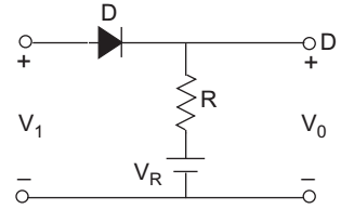
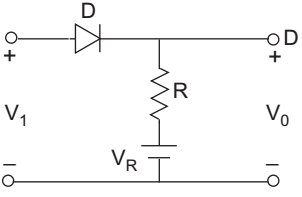
From above circuit it is clear that, the circuit clipps off the input Vi for Vi > VR.Correct Option: A

From above circuit it is clear that, the circuit clipps off the input Vi for Vi > VR.
-
In the circuit the input Vi has positive and negative swings. Vo is the output—
-
View Hint View Answer Discuss in Forum
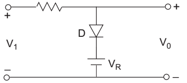
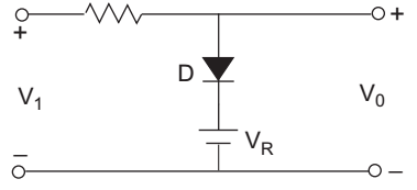
From the given circuit it is clear that the output will appear only when the diode will be in the conducting situation, and it will be possible only when Vi > VR, than V0 = VR.
Hence alternative (C) is the correct answer.Correct Option: C
From the given circuit it is clear that the output will appear only when the diode will be in the conducting situation, and it will be possible only when Vi > VR, than V0 = VR.

Hence alternative (C) is the correct answer.
-
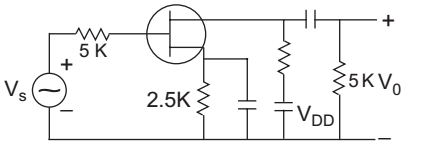
Given gm = 2 mA/V, rd → ∞, |AV| = 
Vo 
is given by— VS
-
View Hint View Answer Discuss in Forum
Given gm = 2 mA/V, rd → ∞, |AV| = 
Vo 
=? VS AV = Vo = gm R′L where R′L = (5 || 5) k = 2.5 k. VS
or AV = 2 × 10– 3 × 2.5 × 103 = 5
Hence alternative (B) is the correct answer.Correct Option: B
Given gm = 2 mA/V, rd → ∞, |AV| = 
Vo 
=? VS AV = Vo = gm R′L where R′L = (5 || 5) k = 2.5 k. VS
or AV = 2 × 10– 3 × 2.5 × 103 = 5
Hence alternative (B) is the correct answer.

