Physical electronics devices and ics miscellaneous
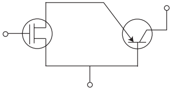
- The gm of the MOS transistor is 4 mA/V and the common base current gain of the bipolar transistor is 0.99. The transconductance of the composite transistor as shown in the figure below will be—
-
View Hint View Answer Discuss in Forum
Emitter current (IE) = gm Vin (in the case of BJT)
α (bipolar) = IC IE
IC = α IE
IC = α. gm Vin …(i)gm (overall) = IC …(ii) Vin
from (i) and (ii)gm (overall) = α·gm Vin Vin
= α. gm = .99 × 4 m A/V
= 3.96 m A/V
Hence alternative (B) is the correct answer.Correct Option: B
Emitter current (IE) = gm Vin (in the case of BJT)
α (bipolar) = IC IE
IC = α IE
IC = α. gm Vin …(i)gm (overall) = IC …(ii) Vin
from (i) and (ii)gm (overall) = α·gm Vin Vin
= α. gm = .99 × 4 m A/V
= 3.96 m A/V
Hence alternative (B) is the correct answer.
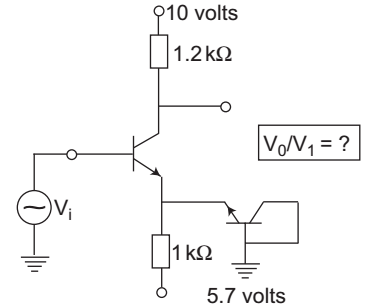
- In figure both transistors are identical and have a high value of beta. Take the do base emitter voltage drop as 0.7 volt and kT/q = 25 mV. The small signal low frequency voltage gain (V0 / Vi) is equal to—
-
View Hint View Answer Discuss in Forum
Given RC = 1.2 kΩ, RE = 1 kΩ from the given
The gain AV = V0 = - RC (by using direct formula) Vi β or AV = 1.2 kΩ = – 1.2 1 kΩ 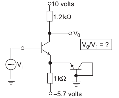
Note: Usually AV = –hfe · RC (1 + hfe) RE + hie
assuming very high gain factor i.e. hfe >> 1 and hie is very small as compare to RE.AV ≈ - RC RE
Hence alternative (D) is the correct answer.Correct Option: D
Given RC = 1.2 kΩ, RE = 1 kΩ from the given
The gain AV = V0 = - RC (by using direct formula) Vi β or AV = 1.2 kΩ = – 1.2 1 kΩ 
Note: Usually AV = –hfe · RC (1 + hfe) RE + hie
assuming very high gain factor i.e. hfe >> 1 and hie is very small as compare to RE.AV ≈ - RC RE
Hence alternative (D) is the correct answer.
- The equivalent circuit of a CE transistor is represented by—
-
View Hint View Answer Discuss in Forum
The equivalent circuit of a CE transistor is represented by figure (B).
Correct Option: B
The equivalent circuit of a CE transistor is represented by figure (B).
- The drain-source output V-I characteristics of an n-channel depletion FET has—
-
View Hint View Answer Discuss in Forum
We know that drain source output V-I characteristics of an n-channel depletion FET is given by relation ID = IDSS 1 – VGS VP 2 from this relation it is clear that IDS will be positive and maximum when VGS = 0, and on increasing VGS the drain current decreases. Hence alternative (B) is the correct answer.
Correct Option: B
We know that drain source output V-I characteristics of an n-channel depletion FET is given by relation ID = IDSS 1 – VGS VP 2 from this relation it is clear that IDS will be positive and maximum when VGS = 0, and on increasing VGS the drain current decreases. Hence alternative (B) is the correct answer.
- The small-signal model of common-base transistor configuration is shown in the given figure.
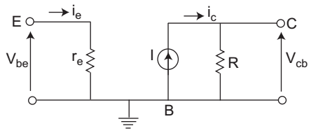
The current source (I) and resistor (R) in the output side are (α is the CB current gain of the transistor)—
-
View Hint View Answer Discuss in Forum
IC = α Ie (since the output current is multiplied by gain factor R0 = re of CB configuration) Hence alternative (D) is the correct answer.
Correct Option: D
IC = α Ie (since the output current is multiplied by gain factor R0 = re of CB configuration) Hence alternative (D) is the correct answer.

