Physical electronics devices and ics miscellaneous
- The change in barrier potential of silicon p-n junction with temperature is—
-
View Hint View Answer Discuss in Forum
The change in barrier potential of a silicon pn-diode with temperature is approximately 2 mV. Therefore alternative (A) is the most correct choice.
Correct Option: A
The change in barrier potential of a silicon pn-diode with temperature is approximately 2 mV. Therefore alternative (A) is the most correct choice.
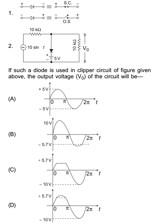
- The equivalent circuits of a diode, during forward biased and reverse biased conditions, are shown in the figure.
-
View Hint View Answer Discuss in Forum
The given circuit (i.e., fig -1)
The given circuit can be redrawn as shown below for first half cycle (i.e., fig -2)
And equivalent circuit for second half cycle is shown below: (i.e., fig -3)From below figure, V0 = 10 × 10 sin t = 5 sin t 10 + 10
Since maximum voltage across at point A may be 5V, hence voltage across the diode always will be less than or equal to zero. So it will be reverse biased always.
Therefore waveform given in alternative (A) is the correct choice.
Correct Option: A
The given circuit (i.e., fig -1)
The given circuit can be redrawn as shown below for first half cycle (i.e., fig -2)
And equivalent circuit for second half cycle is shown below: (i.e., fig -3)From below figure, V0 = 10 × 10 sin t = 5 sin t 10 + 10
Since maximum voltage across at point A may be 5V, hence voltage across the diode always will be less than or equal to zero. So it will be reverse biased always.
Therefore waveform given in alternative (A) is the correct choice.
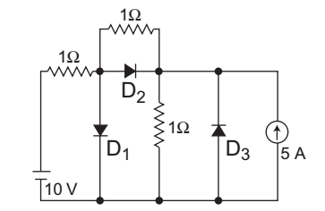
- What are the states of the three ideal diodes of the circuit shown in figure?
-
View Hint View Answer Discuss in Forum
The given circuit (i.e., fig-1)
From given figure are conclude that both D1 and D2 are in forward bias and D3 is in reverse bias. But no current will flow through the diode D2. This is so because current gets shorted path through D1, as shown below (i.e., fig-2)
Hence,
D1 → ON
D2 → OFF
D3 → OFF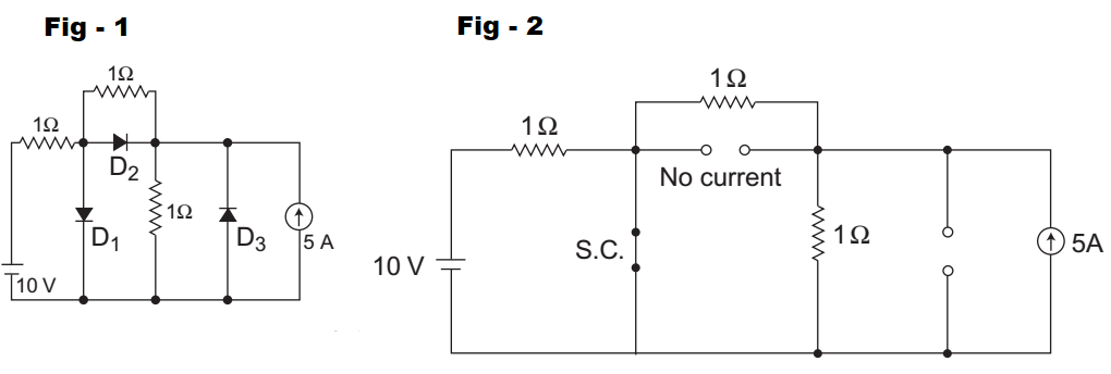
Correct Option: A
The given circuit (i.e., fig-1)
From given figure are conclude that both D1 and D2 are in forward bias and D3 is in reverse bias. But no current will flow through the diode D2. This is so because current gets shorted path through D1, as shown below (i.e., fig-2)
Hence,
D1 → ON
D2 → OFF
D3 → OFF
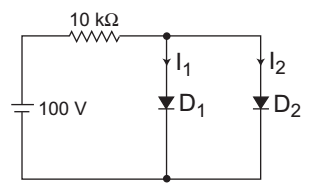
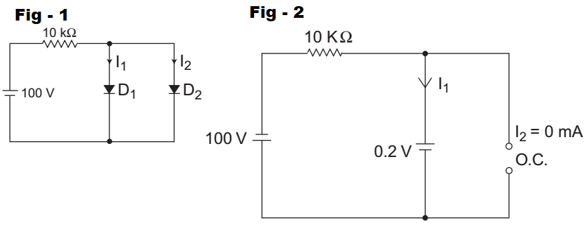
- Each diode in figure can be described by a cut-in voltage and zero resistance. If the cut-in voltage of diode D1 is 0·2V and of diode D2 is 0·6 V, the magnitude of current i1 through D1 is ………… mA and magnitude of current through D2 is ………… mA.
-
View Hint View Answer Discuss in Forum
The given circuit (i.e., fig- 1)
Given that cut-in voltage of diode D1 is 0·2V and D2 is 0·6V. Since the cut-in voltage of diode D1 is 0·2V i.e., less than the cut-in voltage of diode D2 is 0·6V, which prevents the diode D2 turning ‘ON’. There fore the equivalent circuit is given by (i.e., fig- 2)Now, I1 = (100 – 0·2)V = 99·8V 10 KΩ 10 KΩ
= 9·98 mA 10 mA
and I2 = 0 mA
Hence alternative (B) is the correct choice.

Correct Option: B
The given circuit (i.e., fig- 1)
Given that cut-in voltage of diode D1 is 0·2V and D2 is 0·6V. Since the cut-in voltage of diode D1 is 0·2V i.e., less than the cut-in voltage of diode D2 is 0·6V, which prevents the diode D2 turning ‘ON’. There fore the equivalent circuit is given by (i.e., fig- 2)Now, I1 = (100 – 0·2)V = 99·8V 10 KΩ 10 KΩ
= 9·98 mA 10 mA
and I2 = 0 mA
Hence alternative (B) is the correct choice.
- What is the reverse recovery time of a diode when switched from forward bias VF to reverse bias VR?
-
View Hint View Answer Discuss in Forum
Time taken to remove the stored minority carriers is the reverse recovery time of a diode when switched from forward bias VF to reverse bias VR.
Correct Option: A
Time taken to remove the stored minority carriers is the reverse recovery time of a diode when switched from forward bias VF to reverse bias VR.

