Physical electronics devices and ics miscellaneous
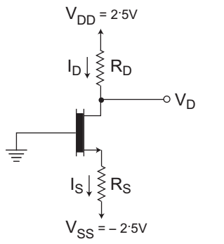
- The NMOS transistor has VT = 0·7 V, µn COX = 100 µA/V2, L = 1 µm, W = 32 µm. If ID = 0·4 mA and VD = 0·5 V. The values of RD and RS are respectively given by—
-
View Hint View Answer Discuss in Forum
The given circuit
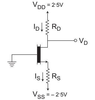
Given, VT = 0·7 V, UnCox = 100 µA/V2
L = 1 µm, W = 32 µm, ID = 0·4 mA, VD = 0·5 V
From figure,or RD = VDD – VD ID = 2·5 – 0·5 = 5 kΩ 0·4 mA
Since, VDS > VGS, this means the NMOS transistor is operating in saturation region.Now, ID = 1 µn COX × W (VGS – VT) 2 2 L
VGS – VT = VDS (Condition for saturation region)
or VGS – VT = 0·5 V
or VGS = 0·5 + VT = 1·2 V
or VG – VS = 1·2 V
or O – VS = 1·2 V or VS = 1·2 VNow, RS = VS – VSS = – 1·2 V – (– 2·5 V) ID 0·4 mA or RS = 1·3 V = 3·25 kΩ 0·4 mA
Hence alternative (A) is the correct choice.Correct Option: C
The given circuit

Given, VT = 0·7 V, UnCox = 100 µA/V2
L = 1 µm, W = 32 µm, ID = 0·4 mA, VD = 0·5 V
From figure,or RD = VDD – VD ID = 2·5 – 0·5 = 5 kΩ 0·4 mA
Since, VDS > VGS, this means the NMOS transistor is operating in saturation region.Now, ID = 1 µn COX × W (VGS – VT) 2 2 L
VGS – VT = VDS (Condition for saturation region)
or VGS – VT = 0·5 V
or VGS = 0·5 + VT = 1·2 V
or VG – VS = 1·2 V
or O – VS = 1·2 V or VS = 1·2 VNow, RS = VS – VSS = – 1·2 V – (– 2·5 V) ID 0·4 mA or RS = 1·3 V = 3·25 kΩ 0·4 mA
Hence alternative (A) is the correct choice.
- Consider the JFET circuit given below—
Current ID is given byAssume ID = 12 1 + VGS 2 mA— 4 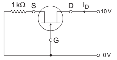
-
View Hint View Answer Discuss in Forum
The given circuit
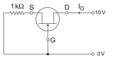
From given circuit VGS = VG – VS = 0 – VS
(Since VG = 0V and VS = IDRS)
or VGS = – IDRS = – ID.1 kΩNow, ID = 12 
1 + VGS 
2 mA 4 Now, ID = 12 
1 - ID 
2 4 or ID = 12 
1 + ID2 – 2.1. ID 
16 4 or ID = 12 
16 + ID2 – 8ID 
16
or 4 ID = 48 + 3 ID2 – 24 ID
or 3 ID2 – 28 ID + 48 = 0or ID = 28 ± √282 – 4 × 3 × 48 2 x 3
ID = 2·26 mA
Hence alternative (A) is the correct choice.
Correct Option: A
The given circuit

From given circuit VGS = VG – VS = 0 – VS
(Since VG = 0V and VS = IDRS)
or VGS = – IDRS = – ID.1 kΩNow, ID = 12 
1 + VGS 
2 mA 4 Now, ID = 12 
1 - ID 
2 4 or ID = 12 
1 + ID2 – 2.1. ID 
16 4 or ID = 12 
16 + ID2 – 8ID 
16
or 4 ID = 48 + 3 ID2 – 24 ID
or 3 ID2 – 28 ID + 48 = 0or ID = 28 ± √282 – 4 × 3 × 48 2 x 3
ID = 2·26 mA
Hence alternative (A) is the correct choice.
- Moor’s law is related to—
-
View Hint View Answer Discuss in Forum
Moor’s law is related to level of integration of MOS devices.
Correct Option: D
Moor’s law is related to level of integration of MOS devices.
- Match List-I (State of operation of an N-MOSFET) with List-II (Required condition) and select the correct answer using the code given below the lists—
List-I
(a) OFF
(b) Linear region
(c) Non-linear
(d) Saturation region
List-II
1. Vgs > Vth and Vds < (Vgs – Vth)
2. Vgs > Vth and Vds > (Vgs – Vth)
3. Vgs > Vth
4. Vgs < Vth
The correct code is—
-
View Hint View Answer Discuss in Forum
N-MOSFET
● OFF → When Vgs < Vth
● Linear region → When Vgs > Vth and Vds < (Vgs – Vth)
● Non-linear → When Vgs > Vth
● Saturation → When Vgs > Vth and Vas > (Vgs region – Vth)Correct Option: B
N-MOSFET
● OFF → When Vgs < Vth
● Linear region → When Vgs > Vth and Vds < (Vgs – Vth)
● Non-linear → When Vgs > Vth
● Saturation → When Vgs > Vth and Vas > (Vgs region – Vth)
- Consider the following statements—
1. The threshold voltage (VT) of a MOS capacitor decreases with increase in gate oxide thickness.
2. The threshold voltage (VT) of a MOS capacitor decreases with increase in substrate doping concentration. Which of the statements given above are correct.
-
View Hint View Answer Discuss in Forum
The threshold voltage of N-channel MOSFET is expressed by
VTN = |Q’SD (max)| - Q’ss + φms + 2φfp Cox Cox
Where, VTN = Threshold voltage for N-MOSFET
Q’ss = Electronic charge perunit area
φms = Work function difference
φfp = Surface potential
e = Charge of electron
∈s = Permitivity
Na = Acceptor ion concentrationCox = ∈ox tox
tox = gate oxide thickness
Thus on increasing gate oxide thickness. Cox decreases which increase threshold voltage, VTN.
And the threshold voltage VTN of a MOS capacitor with increase in substrate doping concentration increases,
since VTN α √Na
Hence alternative (A) is the correct choice.Correct Option: A
The threshold voltage of N-channel MOSFET is expressed by
VTN = |Q’SD (max)| - Q’ss + φms + 2φfp Cox Cox
Where, VTN = Threshold voltage for N-MOSFET
Q’ss = Electronic charge perunit area
φms = Work function difference
φfp = Surface potential
e = Charge of electron
∈s = Permitivity
Na = Acceptor ion concentrationCox = ∈ox tox
tox = gate oxide thickness
Thus on increasing gate oxide thickness. Cox decreases which increase threshold voltage, VTN.
And the threshold voltage VTN of a MOS capacitor with increase in substrate doping concentration increases,
since VTN α √Na
Hence alternative (A) is the correct choice.

