Physical electronics devices and ics miscellaneous
- A material has conductivity of a 10–2 mho/m and a relative permittivity of 4, the frequency at which the conduction current in the medium is equal to the displacement current is—
-
View Hint View Answer Discuss in Forum
NA
Correct Option: A
NA
- The diffusion capacitance of a forward biased p+ – n junction diode with a steady current I depends on—
-
View Hint View Answer Discuss in Forum
The diffusion capacitance of a forward biased p+–n junction is given by
CD = I VT
Where, = Mean life time of charge carriers
I = Forward current
CD = Diffusion capacitance
VT = Volt equivalent of temperature p+ – n → means p-layer is heavily doped than n-layer. It means the current at the junction is entirely due to holes. Thus diffusion capacitance of a forward biased p+ – n junction diode with a steady current I depends on mean life time of the holes.Correct Option: B
The diffusion capacitance of a forward biased p+–n junction is given by
CD = I VT
Where, = Mean life time of charge carriers
I = Forward current
CD = Diffusion capacitance
VT = Volt equivalent of temperature p+ – n → means p-layer is heavily doped than n-layer. It means the current at the junction is entirely due to holes. Thus diffusion capacitance of a forward biased p+ – n junction diode with a steady current I depends on mean life time of the holes.
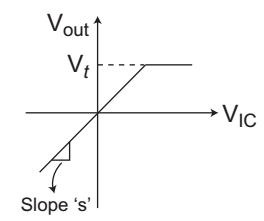
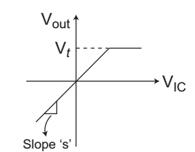
- The figure given below shows the transfer characteristics of which one of the following—

-
View Hint View Answer Discuss in Forum
The given circuit (i.e., fig)
Figure shows the transfer characteristics of Peak clipper.
Correct Option: A
The given circuit (i.e., fig)
Figure shows the transfer characteristics of Peak clipper.
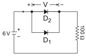
- In the given circuit, D1 is an ideal germanium diode and D2 is a silicon diode having its cut-in voltage as 0·7 V, forward resistance as 20 Ω and reverse saturation current (Is) as 10 nA. What are the values of I and V for this circuit, respectively?

-
View Hint View Answer Discuss in Forum
The given circuit (i.e., fig-1)
Given D1 → Ideal Germanium diode D2 → Silicon diode with
Vr = 0·7V and
Vf = 20Ω and I0 = 10 nA
The equivalent circuit of the given circuit using given information can be redrawn as(i.e., fig-2)From above circuit, V = 0V and I = V loge e 2VT
Hence alternative (A) is the correct choice.

Correct Option: A
The given circuit (i.e., fig-1)
Given D1 → Ideal Germanium diode D2 → Silicon diode with
Vr = 0·7V and
Vf = 20Ω and I0 = 10 nA
The equivalent circuit of the given circuit using given information can be redrawn as(i.e., fig-2)From above circuit, V = 0V and I = V loge e 2VT
Hence alternative (A) is the correct choice.

- Assuming an operating temperature T = 300 K and corresponding VT = 26 mV, what is the change in semiconductor silicon diode forward voltage VD to produce a 10: 1 change in diode current ID, while operating in the forward bias region (<25mA)?
-
View Hint View Answer Discuss in Forum
We know that diode current equation is given by
I = I0 
e V - 1 
VT
[For forward bias]I = I0 
e V 
VT
Since, = 2 for Si diode
Where, I = Forward currentI = I0 
V 
2VT
I0 = Leakage current
V = Applied forward voltage
VT = Volt equivalent of temperature (Given VT = 26 mV)From equation I1 e V1 – V2 I2 2VT Given I1 = 10 then I2 1 10 e V (V = change in forward voltage) 2V2 or 10 loge 10 = V loge e 2VT
or V 2VT loge10
2 × 26 mV × loge10 119·7 mV
Hence alternative (B) is the correct choice.
Correct Option: B
We know that diode current equation is given by
I = I0 
e V - 1 
VT
[For forward bias]I = I0 
e V 
VT
Since, = 2 for Si diode
Where, I = Forward currentI = I0 
V 
2VT
I0 = Leakage current
V = Applied forward voltage
VT = Volt equivalent of temperature (Given VT = 26 mV)From equation I1 e V1 – V2 I2 2VT Given I1 = 10 then I2 1 10 e V (V = change in forward voltage) 2V2 or 10 loge 10 = V loge e 2VT
or V 2VT loge10
2 × 26 mV × loge10 119·7 mV
Hence alternative (B) is the correct choice.

