Physical electronics devices and ics miscellaneous
- The ‘h’ parameter equivalent circuit of a junction transistor is valid for—
-
View Hint View Answer Discuss in Forum
The ‘h’ parameter equivalent circuit of a junction transistor is valid for low frequency, small signal operation only. Hence alternative (C) is the correct answer.
Correct Option: C
The ‘h’ parameter equivalent circuit of a junction transistor is valid for low frequency, small signal operation only. Hence alternative (C) is the correct answer.
- Consider the following statements associated with bipolar junction transistor and junction gate FET—
1. The former has higher input impedance than the latter.
2. The former has higher frequency capability than the latter.
3. The latter has lower noise figure than the former.
4. The latter has higher power rating than the former. Of these statements—
-
View Hint View Answer Discuss in Forum
The main advantage of BJT over FET is that BJT has higher frequency capability that FET. While BJT has higher noise figure than the FET, this is the main disadvantage. Hence alternative (B) is the correct answer.
Correct Option: B
The main advantage of BJT over FET is that BJT has higher frequency capability that FET. While BJT has higher noise figure than the FET, this is the main disadvantage. Hence alternative (B) is the correct answer.
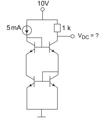
- In figure, all transistors are identical and have a high value of beta (β). The voltage VDC equal to—
-
View Hint View Answer Discuss in Forum
From figure
IE2 = 1 + 2 ≈ 1 as β is of high value. IC3 β 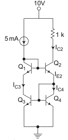
Thus IE2 = IC3
IC3 ≈ 5 mA
and IC2 ≈ IE2
so V0 = VCC – (1 kΩ) × IC2
or V0 = 10 – 1 × 103 × 5 × 10– 3
or V0 = 10 – 5
or V0 = 5 V
Hence alternative (D) is the correct answer.Correct Option: D
From figure
IE2 = 1 + 2 ≈ 1 as β is of high value. IC3 β 
Thus IE2 = IC3
IC3 ≈ 5 mA
and IC2 ≈ IE2
so V0 = VCC – (1 kΩ) × IC2
or V0 = 10 – 1 × 103 × 5 × 10– 3
or V0 = 10 – 5
or V0 = 5 V
Hence alternative (D) is the correct answer.
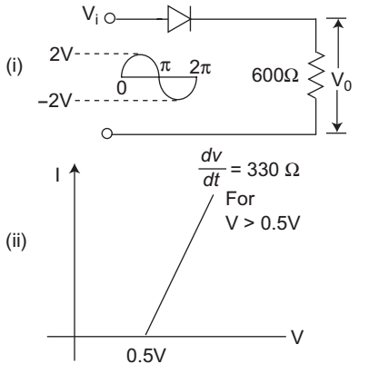
- Consider the circuit shown in Figure (i). If the diode used here has the V-I characteristic as in Figure (ii), then the output waveform V0 is—
-
View Hint View Answer Discuss in Forum
From given figure given that resistance of diode Rf = dv = 300 Ω dI
and the diode will conduct for input voltage greater than 0.5 V.
The complete equivalent circuit of the diode can be given as for the positive half cycle.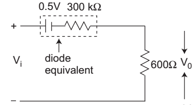 .
.so, V0 = (Vi – 0.5). 600 (600 + 300) or V0 = 1.5 × 600 900
or V0 = 1.0 V
However, for the negative half cycle of the input voltage Vi, the diode is in the non-conduction stage and we get zero output.
Hence alternative (C) is the correct answer.Correct Option: C
From given figure given that resistance of diode Rf = dv = 300 Ω dI
and the diode will conduct for input voltage greater than 0.5 V.
The complete equivalent circuit of the diode can be given as for the positive half cycle. .
.so, V0 = (Vi – 0.5). 600 (600 + 300) or V0 = 1.5 × 600 900
or V0 = 1.0 V
However, for the negative half cycle of the input voltage Vi, the diode is in the non-conduction stage and we get zero output.
Hence alternative (C) is the correct answer.
- A semiconductor is irradiated with light such that carriers are uniformly generated throughout its volume. The semiconductor is n-type with ND = 1019 per cm3. If the excess electron concentration in the steady state is ∆n = 1015 per cm3 and τP = 10 µ sec. [minority carrier liftime] the generation rate due to irradiation—
-
View Hint View Answer Discuss in Forum
We know that
Rate of generation of minority carriers 
100 x 5 dp 
dt = excess hole concentration minority carrier life time
but at equilibrium (steady state)
∆P = ∆ndp = ∆n = 1015 dt τp 10 × 10–6
= 1020 e-h pairs/cm3/sec.
Hence alternative (A) is the correct answer.
Correct Option: A
We know that
Rate of generation of minority carriers 
100 x 5 dp 
dt = excess hole concentration minority carrier life time
but at equilibrium (steady state)
∆P = ∆ndp = ∆n = 1015 dt τp 10 × 10–6
= 1020 e-h pairs/cm3/sec.
Hence alternative (A) is the correct answer.

