Analog electronics circuits miscellaneous
- An amplifier has an open-loop gain of 100, and its lower and upper-cut -off frequency of 100 Hz and 100 kHz, respectively. A feedback network with a feedback factor of 0.99 is connected to the amplifier. The new lower and upper-cut-off frequencies are at___and ___
-
View Hint View Answer Discuss in Forum
Af = A = 100 = 1 1 + Aβ 1 + 100 × 0·99
f*H = fH. (1 + Aβ) = 100 × 103 (1 + 0.99 × 100)
= 10 MHzf*L = fL = 100 = 1 = 1 Hz. 1 + Aβ (1 + 100 × 0·99) Correct Option: A
Af = A = 100 = 1 1 + Aβ 1 + 100 × 0·99
f*H = fH. (1 + Aβ) = 100 × 103 (1 + 0.99 × 100)
= 10 MHzf*L = fL = 100 = 1 = 1 Hz. 1 + Aβ (1 + 100 × 0·99)
- A power amplifier delivers 50 W output at 50% efficiency. The ambient temperature is 25° C. If the maximum allowable junction temperature is 150° C, then the maximum thermal resistance Qjc that can be tolerated is:
-
View Hint View Answer Discuss in Forum
PD = P0 × efficiency
= dissipated power at the outputPD = 50 × 50 = 25 W 100
Given that, Ti = 150° C
TA = 25°C
Now,PD = Ti – TA Qjc
where, Ti = instantaneous temperature
TA = ambient temp.Qjc = Ti – TA = 150 – 25 = 5° C/W PD 25
Qjc = thermal resistanceCorrect Option: C
PD = P0 × efficiency
= dissipated power at the outputPD = 50 × 50 = 25 W 100
Given that, Ti = 150° C
TA = 25°C
Now,PD = Ti – TA Qjc
where, Ti = instantaneous temperature
TA = ambient temp.Qjc = Ti – TA = 150 – 25 = 5° C/W PD 25
Qjc = thermal resistance
- An R–C coupled amplifier is assumed to have a singlepole low frequency transfer function. The Maximum lower-cut -off frequency allowed for the amplifier to pass 50 Hz square wave with no more than 100% till is:
-
View Hint View Answer Discuss in Forum
Fractional tilt = πfL f
where, fL = Lower cut-off frequency
f = applied signal frequencyor fL = f × fractional tilt π or fL = 50 × 10/100 3·14
= 1.59 HzCorrect Option: C
Fractional tilt = πfL f
where, fL = Lower cut-off frequency
f = applied signal frequencyor fL = f × fractional tilt π or fL = 50 × 10/100 3·14
= 1.59 Hz
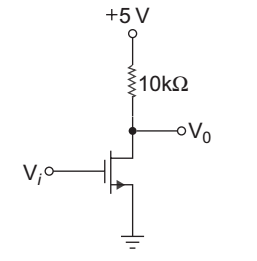
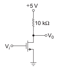
- For the circuit shown below the transistor parameter are VTN = 0.8 V and kn = 30 µ A/V2. If output voltage is V0 = 0.1 V, when input voltage is Vi = 4.2 V, the required transistor width-to-length ratio is:

-
View Hint View Answer Discuss in Forum
Given that
VTN = 0.8 V
k′n = 30 µA/V2
V0 = 0.1 V
Vi = 4.2 V
From fig. VGS = Vi = 4.2 Vand ID = 5 – V0 = 5 – 0·1 10 kΩ 10 × 103 = 4·9 = 0.49 mA 10 × 103 Again ID = 1 . k'n 
W 
(VGS–VTN)2 2 L
= 0.49 × 10⁻³ or 0.49 × 10–3
= 1 × 30 × 10–6. 
W 
. (4.2 – 0.8)2 2 L or 
W 
= 0·49 × 103 = 2.825 L 15 × (3·4)2
Hence alternative (D) is the correct choice.
Correct Option: D
Given that
VTN = 0.8 V
k′n = 30 µA/V2
V0 = 0.1 V
Vi = 4.2 V
From fig. VGS = Vi = 4.2 Vand ID = 5 – V0 = 5 – 0·1 10 kΩ 10 × 103 = 4·9 = 0.49 mA 10 × 103 Again ID = 1 . k'n 
W 
(VGS–VTN)2 2 L
= 0.49 × 10⁻³ or 0.49 × 10–3
= 1 × 30 × 10–6. 
W 
. (4.2 – 0.8)2 2 L or 
W 
= 0·49 × 103 = 2.825 L 15 × (3·4)2
Hence alternative (D) is the correct choice.
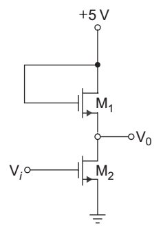
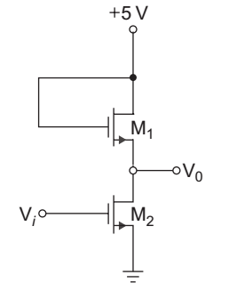
- The transistors in the circuit of given below have parameter VTN = 0.8 V, kn = 40 µA/V2 and λ = 0. The width-to-length ratio of M2 is

W 
= 1. L 2
If V0 = 0.10 V when Vi = 5 V, then
W 
for M1 is: L 1 
-
View Hint View Answer Discuss in Forum
Given that
VTN = 0.84
k′n = 40 µA/V2
W 
= 1 L 2
V0 = 0.10 V
Vi = 5 V
For transistor M2
VDS = 0.1 V
VGS1 = Vi = 5 V
∴ VDS < VGS – VTN, therefore the transistor M2 work in the linear region
ID2 = ID1 = IDID2 = 1 k'n 
W 
. [2(VGS2 – VTn)VDS2 – V2DS2 ]…(A) 2 L 2 ID1 = 1 kn′ 
W 
(VGS1 – VTn)2 …(B) 2 L 1
solving equation (A) and (B)1. (5 – 0.1 – 0.8)2 = 
W 
[2 . (5 – 0.8) 0.1 – (0.1)2] L 1 (4.1)2 = 
W 
[0·84 – 0.01] L 1 or = 
W 
= (4.1)2 = 20.25 L 1 0·83
Hence alternative (D) is the correct choice.
Correct Option: D
Given that
VTN = 0.84
k′n = 40 µA/V2
W 
= 1 L 2
V0 = 0.10 V
Vi = 5 V
For transistor M2
VDS = 0.1 V
VGS1 = Vi = 5 V
∴ VDS < VGS – VTN, therefore the transistor M2 work in the linear region
ID2 = ID1 = IDID2 = 1 k'n 
W 
. [2(VGS2 – VTn)VDS2 – V2DS2 ]…(A) 2 L 2 ID1 = 1 kn′ 
W 
(VGS1 – VTn)2 …(B) 2 L 1
solving equation (A) and (B)1. (5 – 0.1 – 0.8)2 = 
W 
[2 . (5 – 0.8) 0.1 – (0.1)2] L 1 (4.1)2 = 
W 
[0·84 – 0.01] L 1 or = 
W 
= (4.1)2 = 20.25 L 1 0·83
Hence alternative (D) is the correct choice.

