Analog electronics circuits miscellaneous
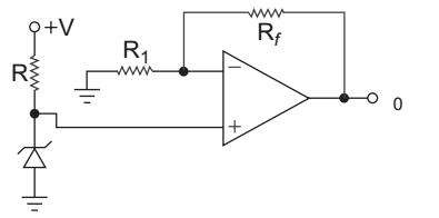
- The circuit shown below:

-
View Hint View Answer Discuss in Forum
In the given circuit zener diode is connected at the non-inverting terminal. Hence circuit represents non-inverting time reference voltage.
Correct Option: B
In the given circuit zener diode is connected at the non-inverting terminal. Hence circuit represents non-inverting time reference voltage.

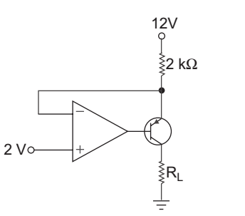
- A circuit shown below. The largest value of RL that can be used is:
-
View Hint View Answer Discuss in Forum
Since transistor in the saturation. op-amp having, Rf = 0
Vo = 2 
1 + Rf 
= 2 V R1
Negative voltage drop between base and collector terminal due to virtual ground,
VA = 2 Vso, current in 2 kΩ resistor = 12 – 2 = 5 mA = I 2 kΩ
Now, since voltage at C is 2 V
so, 2 = I × RL
2 = 5 × 10⁻³. RL
or RL = 400 Ω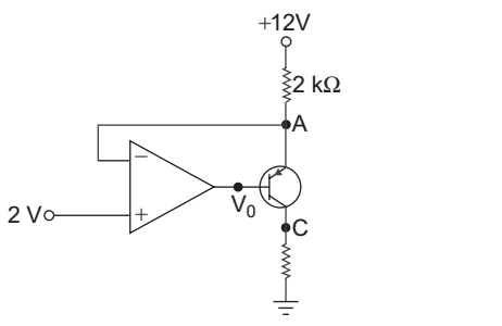
Correct Option: B
Since transistor in the saturation. op-amp having, Rf = 0
Vo = 2 
1 + Rf 
= 2 V R1
Negative voltage drop between base and collector terminal due to virtual ground,
VA = 2 Vso, current in 2 kΩ resistor = 12 – 2 = 5 mA = I 2 kΩ
Now, since voltage at C is 2 V
so, 2 = I × RL
2 = 5 × 10⁻³. RL
or RL = 400 Ω
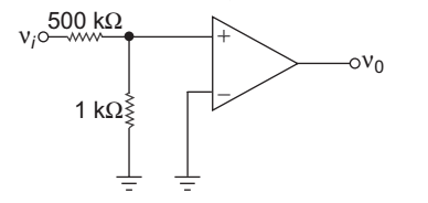
- For the circuit shown below, the output voltage is ν0 = 2.5 V in response to input voltage νi = 5 V. The finite open-loop differential gain of the op-amp is:
-
View Hint View Answer Discuss in Forum
From figure
VA = Vi × 1 1 + 500 VA = Vi 501 and Vo = Aod. VA = Aod. Vi 501 or Aod = 501. V0 = 501 × 2·5 = 250.5 V1 5 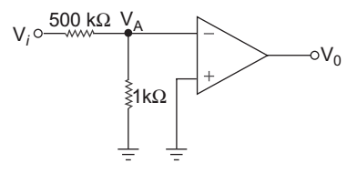
Correct Option: B
From figure
VA = Vi × 1 1 + 500 VA = Vi 501 and Vo = Aod. VA = Aod. Vi 501 or Aod = 501. V0 = 501 × 2·5 = 250.5 V1 5 
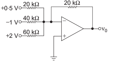
- In the circuit shown below the output voltage ν0 is:
-
View Hint View Answer Discuss in Forum
Vo = – 0.5 20 + 1 
20 
– 2 
20 
20 40 60
= – 0.5 + 0.5 – 0.667
= – 0.667 V
Correct Option: C
Vo = – 0.5 20 + 1 
20 
– 2 
20 
20 40 60
= – 0.5 + 0.5 – 0.667
= – 0.667 V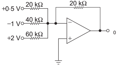
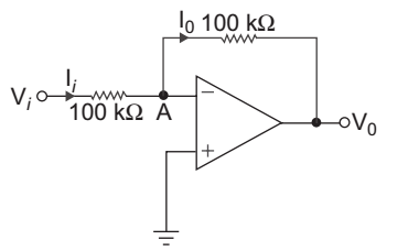
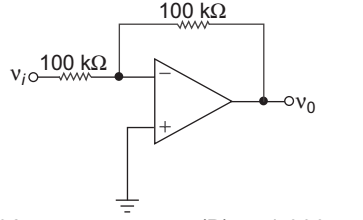
- For the op-amp shown in fig below open loop differential gain is Aod = 103. The output voltage ν0 for νi = 2 V is:
-
View Hint View Answer Discuss in Forum
KCL at node A.
I1 = I0I1 = Vi – VA 100 kΩ I0 = VA – V0 100 kΩ given, Aod = 103 = – V0 and Vi = 2 V VA or VA = –V0 103
Now Vi – VA = VA – Vo
or Vi + Vo = 2 VAor Vi + Vo = 2 · 
–V0 
103 or 2 + Vo = –2V0 103 or Vo + 2V0 = – 2 103 or Vo = –2 × 103 = – 1.996 V (103 + 2)
Hence alternative (A) is the correct choice
Correct Option: A
KCL at node A.
I1 = I0I1 = Vi – VA 100 kΩ I0 = VA – V0 100 kΩ given, Aod = 103 = – V0 and Vi = 2 V VA or VA = –V0 103
Now Vi – VA = VA – Vo
or Vi + Vo = 2 VAor Vi + Vo = 2 · 
–V0 
103 or 2 + Vo = –2V0 103 or Vo + 2V0 = – 2 103 or Vo = –2 × 103 = – 1.996 V (103 + 2)
Hence alternative (A) is the correct choice