Analog electronics circuits miscellaneous
- An R–C coupled amplifier is assumed to have a singlepole low frequency transfer function. The Maximum lower-cut -off frequency allowed for the amplifier to pass 50 Hz square wave with no more than 100% till is:
-
View Hint View Answer Discuss in Forum
Fractional tilt = πfL f
where, fL = Lower cut-off frequency
f = applied signal frequencyor fL = f × fractional tilt π or fL = 50 × 10/100 3·14
= 1.59 HzCorrect Option: C
Fractional tilt = πfL f
where, fL = Lower cut-off frequency
f = applied signal frequencyor fL = f × fractional tilt π or fL = 50 × 10/100 3·14
= 1.59 Hz
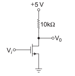
- For the circuit shown below the transistor parameter are VTN = 0.8 V and kn = 30 µ A/V2. If output voltage is V0 = 0.1 V, when input voltage is Vi = 4.2 V, the required transistor width-to-length ratio is:
-
View Hint View Answer Discuss in Forum
Given that
VTN = 0.8 V
k′n = 30 µA/V2
V0 = 0.1 V
Vi = 4.2 V
From fig. VGS = Vi = 4.2 Vand ID = 5 – V0 = 5 – 0·1 10 kΩ 10 × 103 = 4·9 = 0.49 mA 10 × 103 Again ID = 1 . k'n 
W 
(VGS–VTN)2 2 L
= 0.49 × 10⁻³ or 0.49 × 10–3
= 1 × 30 × 10–6. 
W 
. (4.2 – 0.8)2 2 L or 
W 
= 0·49 × 103 = 2.825 L 15 × (3·4)2
Hence alternative (D) is the correct choice.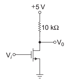
Correct Option: D
Given that
VTN = 0.8 V
k′n = 30 µA/V2
V0 = 0.1 V
Vi = 4.2 V
From fig. VGS = Vi = 4.2 Vand ID = 5 – V0 = 5 – 0·1 10 kΩ 10 × 103 = 4·9 = 0.49 mA 10 × 103 Again ID = 1 . k'n 
W 
(VGS–VTN)2 2 L
= 0.49 × 10⁻³ or 0.49 × 10–3
= 1 × 30 × 10–6. 
W 
. (4.2 – 0.8)2 2 L or 
W 
= 0·49 × 103 = 2.825 L 15 × (3·4)2
Hence alternative (D) is the correct choice.
- The transistors in the circuit of given below have parameter VTN = 0.8 V, kn = 40 µA/V2 and λ = 0. The width-to-length ratio of M2 is

W 
= 1. L 2
If V0 = 0.10 V when Vi = 5 V, then
W 
for M1 is: L 1 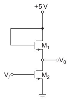
-
View Hint View Answer Discuss in Forum
Given that
VTN = 0.84
k′n = 40 µA/V2
W 
= 1 L 2
V0 = 0.10 V
Vi = 5 V
For transistor M2
VDS = 0.1 V
VGS1 = Vi = 5 V
∴ VDS < VGS – VTN, therefore the transistor M2 work in the linear region
ID2 = ID1 = IDID2 = 1 k'n 
W 
. [2(VGS2 – VTn)VDS2 – V2DS2 ]…(A) 2 L 2 ID1 = 1 kn′ 
W 
(VGS1 – VTn)2 …(B) 2 L 1
solving equation (A) and (B)1. (5 – 0.1 – 0.8)2 = 
W 
[2 . (5 – 0.8) 0.1 – (0.1)2] L 1 (4.1)2 = 
W 
[0·84 – 0.01] L 1 or = 
W 
= (4.1)2 = 20.25 L 1 0·83
Hence alternative (D) is the correct choice.
Correct Option: D
Given that
VTN = 0.84
k′n = 40 µA/V2
W 
= 1 L 2
V0 = 0.10 V
Vi = 5 V
For transistor M2
VDS = 0.1 V
VGS1 = Vi = 5 V
∴ VDS < VGS – VTN, therefore the transistor M2 work in the linear region
ID2 = ID1 = IDID2 = 1 k'n 
W 
. [2(VGS2 – VTn)VDS2 – V2DS2 ]…(A) 2 L 2 ID1 = 1 kn′ 
W 
(VGS1 – VTn)2 …(B) 2 L 1
solving equation (A) and (B)1. (5 – 0.1 – 0.8)2 = 
W 
[2 . (5 – 0.8) 0.1 – (0.1)2] L 1 (4.1)2 = 
W 
[0·84 – 0.01] L 1 or = 
W 
= (4.1)2 = 20.25 L 1 0·83
Hence alternative (D) is the correct choice.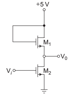
- In the circuit given below the transistor parameters are
VTN = 1 V, and kn = 36 µA/V2. If ID = 0.5 mA, V1 = 5 V and V2 = 2 V then the width-to-length ratio
i.e. W 
required in each transistor is L 
W 

W 

W 
L 1 L 2 L 3 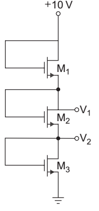
-
View Hint View Answer Discuss in Forum
For each transistor M1, M2 and M2
VGS = VDS i.e. VDS > VGS – VTN
Therefore all the transistor are in saturation Given that
VTN = 1 V
k′n = 36 µA/V2
ID = 0.5 mA
V1 = 5 VS V2 = 2 V
For transistor M3
V2 = 2V = VGS3
ID = 0.5 × 10–3= 1 36 × 10–6 
W 
. (2 – 1)2 2 L 3 after simplifying we get 
W 
= 27.8 L 3
For transistor M2,
VGS2 = V1 – V2 = 5 – 2 = 3 V
ID = 0.5 × 10–3= 36 × 10–6 
W 
(3 – 1)2 L 2 or 
W 
= 6.94 L 2
For transistor M1
VGS1 = 10 – V1 = 10 – 5 = 5 V
ID = 0.5 × 10–3= 1 36 × 10–6 
W 
. (5 – 1)2 2 L 1 or 
W 
= 1.74 L 1
Hence alternative (A) is the correct choice.Correct Option: A
For each transistor M1, M2 and M2
VGS = VDS i.e. VDS > VGS – VTN
Therefore all the transistor are in saturation Given that
VTN = 1 V
k′n = 36 µA/V2
ID = 0.5 mA
V1 = 5 VS V2 = 2 V
For transistor M3
V2 = 2V = VGS3
ID = 0.5 × 10–3= 1 36 × 10–6 
W 
. (2 – 1)2 2 L 3 after simplifying we get 
W 
= 27.8 L 3
For transistor M2,
VGS2 = V1 – V2 = 5 – 2 = 3 V
ID = 0.5 × 10–3= 36 × 10–6 
W 
(3 – 1)2 L 2 or 
W 
= 6.94 L 2
For transistor M1
VGS1 = 10 – V1 = 10 – 5 = 5 V
ID = 0.5 × 10–3= 1 36 × 10–6 
W 
. (5 – 1)2 2 L 1 or 
W 
= 1.74 L 1
Hence alternative (A) is the correct choice.
Direction: Consider the circuit shown below:
The both transistor have parameter as follows:
VTN = 0.8 V, kn = 30 ΩA/V2

-
If the ratio is 
W 
= 40 and 
W 
= 15, then V0 is: L 1 L 2
-
View Hint View Answer Discuss in Forum
According to question

W 
= 40 and 
W 
= 15 L 1 L 2
Again
Kn1 (VGS1 – VTN1 )2=Kn2 (VGS2 – VTN2 )2
40 (VGS1 – 0.8)2 = 15 (VGS2 – 0.8)2 `…(A)
VGS1 + VGS2 = 5 …(B)
from (A) and (B)
40 (VGS1 – 0.8)2 = 15 (5 – VGS1 – 0.8)2
8 [V2GS1 +.64 –1.6 VGS1] = 3 [17.64 + V2GS1 –8 VGS1]
5 V2GS1 + 11.2 VGS1 – 47.8 = 0
VGS1 = 2.09
V0 = 5 – VGS1
= 5 – 2.09 = 2.91 V
Correct Option: A
According to question

W 
= 40 and 
W 
= 15 L 1 L 2
Again
Kn1 (VGS1 – VTN1 )2=Kn2 (VGS2 – VTN2 )2
40 (VGS1 – 0.8)2 = 15 (VGS2 – 0.8)2 `…(A)
VGS1 + VGS2 = 5 …(B)
from (A) and (B)
40 (VGS1 – 0.8)2 = 15 (5 – VGS1 – 0.8)2
8 [V2GS1 +.64 –1.6 VGS1] = 3 [17.64 + V2GS1 –8 VGS1]
5 V2GS1 + 11.2 VGS1 – 47.8 = 0
VGS1 = 2.09
V0 = 5 – VGS1
= 5 – 2.09 = 2.91 V

