Analog electronics circuits miscellaneous
- The emitter resistance in a differential amplifier is used to:
-
View Hint View Answer Discuss in Forum
The main purpose of emitter resistance in a differential amplifier made larger to maintain the proper quiescent current, in order to provide the stability to the transistor, or in other words to bias the transistor is active region.
Correct Option: C
The main purpose of emitter resistance in a differential amplifier made larger to maintain the proper quiescent current, in order to provide the stability to the transistor, or in other words to bias the transistor is active region.
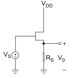
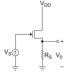
- In the FET circuit shown below:
The nature of feedback and impedance levels are given in the following statements:
(i) It is current series feedback
(ii) It is voltage series feedback
(iii) The input resistance is increased by feedback.
(iv) The output resistance is increased. The correct statements are:
-
View Hint View Answer Discuss in Forum
Since the voltage is feedback therefore the type of feedback is voltage feedback and since the feedback is in loop form.
Hence the circuit represents voltage-series feedback.
In voltage-series feedback input impedance after feedback, is increases and output resistance decreases.
Hence alternative (B) is the correct choice.
Correct Option: B
Since the voltage is feedback therefore the type of feedback is voltage feedback and since the feedback is in loop form.
Hence the circuit represents voltage-series feedback.
In voltage-series feedback input impedance after feedback, is increases and output resistance decreases.
Hence alternative (B) is the correct choice.
- An amplifier has a bandwidth of 20 kHz and a mid band gain of 50 without feedback. If a negative feedback of 1% is applied, then bandwidth with feedback is:
-
View Hint View Answer Discuss in Forum
Given, BW = 20 kHz
A = 50
B = 1% = 0.01
BW* = BW (1 + Aβ)
(∴ after feedback bandwidth increases)
or BW* = 20 kHz (1 + 50 × 0.01)
BW* = 30 kHzCorrect Option: B
Given, BW = 20 kHz
A = 50
B = 1% = 0.01
BW* = BW (1 + Aβ)
(∴ after feedback bandwidth increases)
or BW* = 20 kHz (1 + 50 × 0.01)
BW* = 30 kHz
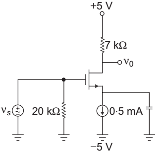
- Consider the common-source circuit with source bypass capacitor. The signal frequency is sufficiently large. The transistor parameters are VTN = 0.8 V, kn = 1 mA/V2. The voltage gain is:

-
View Hint View Answer Discuss in Forum
NA
Correct Option: B
NA
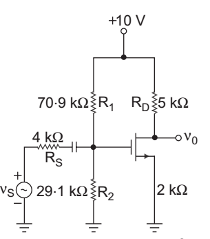
Direction: Consider the common source amplifier shown below. The transistor parameter are VTN = 1.5 V, Kn = 0.5 mA/ V2, and λ = 0.01 V– 1. The resistance of source is RS = 4 kΩ.

- The amplifier output resistance is:
-
View Hint View Answer Discuss in Forum
From small-signal equivalent circuit shown in fig.
Ri = R1 || R2 = 70.9 || 29.1 = 20.6 kΩ
Correct Option: A
From small-signal equivalent circuit shown in fig.
Ri = R1 || R2 = 70.9 || 29.1 = 20.6 kΩ

