Analog electronics circuits miscellaneous
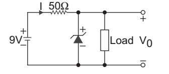
- A zener diode in the circuit shown below, has a knee current of 5 mA, and a maximum allowed power dissipation of 300 mW. What are the minimum and maximum load current that can be drawn safely from the circuit, keeping the output voltage V0 at 6 V?
-
View Hint View Answer Discuss in Forum
Given, IZ (min) = 5 mA
V0 = 6 V = Vz
(according to given condition).
Maximum power dissipation means maximum zener current
i.e. Iz (max) = Pmax V = 300 mW 6 V = 50 mA
from figure
I = Vin – Vz 50 = 9 – 6 50 = 60 mA
and I = IZ + IL
IL (min) = I – Iz (max) = 60 – 50 = 10 mA
IL (max) = I – Iz (min) = 60 – 5 = 55 mA
Hence alternative (C) is the correct choice.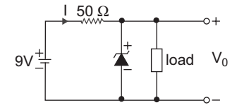
Correct Option: C
Given, IZ (min) = 5 mA
V0 = 6 V = Vz
(according to given condition).
Maximum power dissipation means maximum zener current
i.e. Iz (max) = Pmax V = 300 mW 6 V = 50 mA
from figure
I = Vin – Vz 50 = 9 – 6 50 = 60 mA
and I = IZ + IL
IL (min) = I – Iz (max) = 60 – 50 = 10 mA
IL (max) = I – Iz (min) = 60 – 5 = 55 mA
Hence alternative (C) is the correct choice.
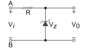
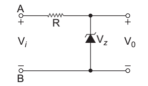
- In order to obtain a 12-V stabilized supply from the current shown in figure below, the input to terminals A and B should be:
-
View Hint View Answer Discuss in Forum
Input voltage should be greater than 12 V to allow for drop across R. Since Zener diode always work in reverse - biased mode. Terminal A should obviously, be positive.
Correct Option: D
Input voltage should be greater than 12 V to allow for drop across R. Since Zener diode always work in reverse - biased mode. Terminal A should obviously, be positive.

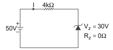
- The current flowing through the zener diode of figure below is:
-
View Hint View Answer Discuss in Forum
From given figure
I = 50 – Vz = 50 – 30 R 4 × 10³
or I = 5 × 10⁻³
or I = 5 mA.
Correct Option: A
From given figure
I = 50 – Vz = 50 – 30 R 4 × 10³
or I = 5 × 10⁻³
or I = 5 mA.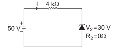
- In the case of self Biasing or potential divider biasing, for good stability factor:
-
View Hint View Answer Discuss in Forum
The stability factor,
S = β + 1(1 + RB/RE) → (A) 1 + β + RB/RE where, RB = R1.R2 R1 + R2
RE = emitter resistance
β = transistor gain
from relation we conclude that for good bias stability i.e. lower value of stability factor S, RB << RE.
Therefore alternative (B) is the correct choice.Correct Option: B
The stability factor,
S = β + 1(1 + RB/RE) → (A) 1 + β + RB/RE where, RB = R1.R2 R1 + R2
RE = emitter resistance
β = transistor gain
from relation we conclude that for good bias stability i.e. lower value of stability factor S, RB << RE.
Therefore alternative (B) is the correct choice.
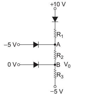
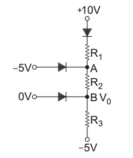
- The cutin voltage for each diode shown below Vγ = 0.6 V. Each diode current is 0.5
-
View Hint View Answer Discuss in Forum
From figure
VA = 5 – 0.6 = 4.4 V
VB = 0 – 0.6 = – 0.6 VR1 = 10 – 0.6 – 4.4 = 10 kΩ 0.5 × 10⁻³ R2 = VA – VB = 4·4 – (0·6) = 5 kΩ 1 × 10⁻³ 1 × 10⁻³ R3 = VB – (–5) = –0.6 + 5 = 4.6 = 2.93 kΩ 1.5 × 10⁻³ 1.5 × 10⁻³ 1.5 × 10⁻³ 
Correct Option: A
From figure
VA = 5 – 0.6 = 4.4 V
VB = 0 – 0.6 = – 0.6 VR1 = 10 – 0.6 – 4.4 = 10 kΩ 0.5 × 10⁻³ R2 = VA – VB = 4·4 – (0·6) = 5 kΩ 1 × 10⁻³ 1 × 10⁻³ R3 = VB – (–5) = –0.6 + 5 = 4.6 = 2.93 kΩ 1.5 × 10⁻³ 1.5 × 10⁻³ 1.5 × 10⁻³ 