Power electronics and drives miscellaneous
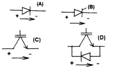
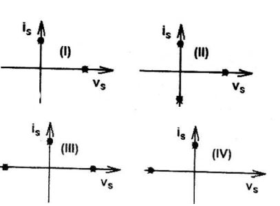
- Match the switch arrangements on the top row to the steady-state V-I characteristics on the lower row. The steady state operating points are shown by large black dots.


-
View Hint View Answer Discuss in Forum

Negative voltage, current = 0Correct Option: C

Negative voltage, current = 0
- In the chopper circuit shown, the main thyristor (TM) is operated at a duty ratio of 0.8 which is
much larger the commutation interval. If the maximum allowable reapplied dv on TM dt
is 50 V/μs, what should be the theoretical minimum value of C1? Assume current ripple through L0 to be negligible.
-
View Hint View Answer Discuss in Forum
I0 = 100 = 12.5 amp 0.8
Duty ratio of TM = 0.8
∴ Current through M, IM = 12.5 × 0.8 = 10ANow IM = C dVM dt ∴ 10 = C × 50 10-6 or C = 50 × 10-6 = 0.2 μF 10
Correct Option: A
I0 = 100 = 12.5 amp 0.8
Duty ratio of TM = 0.8
∴ Current through M, IM = 12.5 × 0.8 = 10ANow IM = C dVM dt ∴ 10 = C × 50 10-6 or C = 50 × 10-6 = 0.2 μF 10
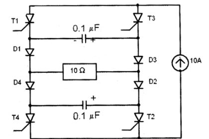
- The Current Source Inverter shown in the figure given below is operated by alternately turning on thyristor pairs (T1, T2) and (T3, T4). If load is purely resistive, then theoretical maximum output frequency obtainable will be

-
View Hint View Answer Discuss in Forum
Let T3 and T4 already conducting at t = 0
Now, trigger T1 and T2, so T3, T4 force commutated.
Now capacitor start to discharge, becomes zero. Now charge with opposite polarityAt t = T , trigger T3, T4 2
So T2, T1 force commutated.
Now capacitor start to discharge, becomes zero and now charge with positive polarity
This completes one cycle
Time constant, = τ = RC = 0.5μs
∴ Total τ = 4 × τ = 4 × 0.5 μs = 2 μs∴ f = 1 = 1 = 500 kHz T 2 × 10⁻⁶ Correct Option: C
Let T3 and T4 already conducting at t = 0
Now, trigger T1 and T2, so T3, T4 force commutated.
Now capacitor start to discharge, becomes zero. Now charge with opposite polarityAt t = T , trigger T3, T4 2
So T2, T1 force commutated.
Now capacitor start to discharge, becomes zero and now charge with positive polarity
This completes one cycle
Time constant, = τ = RC = 0.5μs
∴ Total τ = 4 × τ = 4 × 0.5 μs = 2 μs∴ f = 1 = 1 = 500 kHz T 2 × 10⁻⁶
- An SCR is considered to be a semi-controlled device because
-
View Hint View Answer Discuss in Forum
NA
Correct Option: C
NA
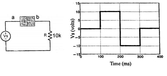
- The following circuit has a source voltage Vs as shown in the graph. The current through the circuit is also shown.


The element connected between a and b could be
-
View Hint View Answer Discuss in Forum
When a forward biased diode is reverse biased, initially it conducts due to the flow of stored charges. After some ti me it goes int o nonconducting state.
Alternately
For 0 < t < 100 ms, Vs = 0,
is = 0; diode not conduct
For 100 < t < 200 ms, Vs = 10V,i = 10 = 1 mA ; diode conducts 10K
For 200 < t < 300 ms, Vs = – 10V, i = 0; diode reverse bias
current is zero after small reverse recovery time.
For 300 < t < 400 ms, Vs = 0;
i = 0; diode not conductCorrect Option: A
When a forward biased diode is reverse biased, initially it conducts due to the flow of stored charges. After some ti me it goes int o nonconducting state.
Alternately
For 0 < t < 100 ms, Vs = 0,
is = 0; diode not conduct
For 100 < t < 200 ms, Vs = 10V,i = 10 = 1 mA ; diode conducts 10K
For 200 < t < 300 ms, Vs = – 10V, i = 0; diode reverse bias
current is zero after small reverse recovery time.
For 300 < t < 400 ms, Vs = 0;
i = 0; diode not conduct

