Advanced Microprocessors
- Match each of the items a, b and c on the left with an approximate item on the right—
(a) A shift register can be used (1) for code conversion (b) A multiplexer can be used (2) to generate memory chip to select (c) A decoder can be used (3) for parallel-to-serial conversion (4) as a many to one switch (5) for analog to digital conversion
-
View Hint View Answer Discuss in Forum
NA
Correct Option: B
NA
- For a MOD-12 counter, the Flip-Flop has a tpd = 60 ns. The NAND gate has a tpd of 25 ns. The maximum clock frequency is given by—
-
View Hint View Answer Discuss in Forum
We know that Maximum frequency is given by
fmax ≤ 1 ts + n tPd
where, n = no. of flip-flop
ts = propagation delay of gate
t Pd = propagation delay of flip-flop.
For Mod-12 counter we require 4 flip-flopfmax ≤ 1 (25 × 10−9 + 4 × 60 × 10−9)
or fmax ≤ 3·774 MHz
So, maximum frequency = 3·774 MHz
Hence alternative (C) is the correct answerCorrect Option: C
We know that Maximum frequency is given by
fmax ≤ 1 ts + n tPd
where, n = no. of flip-flop
ts = propagation delay of gate
t Pd = propagation delay of flip-flop.
For Mod-12 counter we require 4 flip-flopfmax ≤ 1 (25 × 10−9 + 4 × 60 × 10−9)
or fmax ≤ 3·774 MHz
So, maximum frequency = 3·774 MHz
Hence alternative (C) is the correct answer
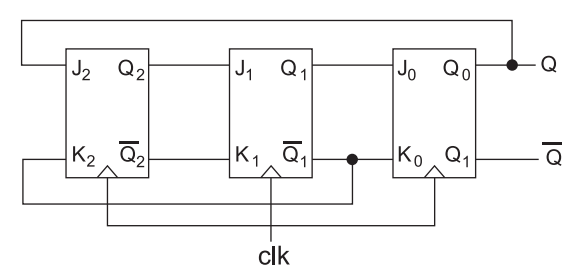
- The divide by N counter is shown in figure. If initially Q0 = 1, Q.1 = 1, Q2 = 0. What is a value of N?
-
View Hint View Answer Discuss in Forum
Given circuit arrangement

From given circuit arrangement, we get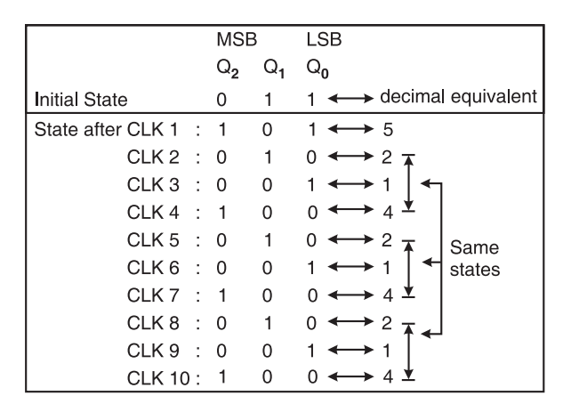
i.e., After first CLK we get 2 → 1 → 4 again and again. Thus we can conclude that the given arrangement is known as Mod–3 counter. Hence alternative (D) is the correct choice.Correct Option: D
Given circuit arrangement
From given circuit arrangement, we get
i.e., After first CLK we get 2 → 1 → 4 again and again. Thus we can conclude that the given arrangement is known as Mod–3 counter. Hence alternative (D) is the correct choice.
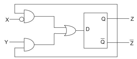
- A sequential circuit using D flip-flop and logic gates is shown where X and Y are inputs and Z is output. The circuit is—
-
View Hint View Answer Discuss in Forum
For D to JK conversion
Qn + 1 = JQ + KQ …(i)
But according to the given figure
Z= XQ + YQ …(ii)
comparing eqn. (i) and (ii), we get
⇒ X = K and Y = J
Hence alternative (D) is the correct answer.Correct Option: D
For D to JK conversion
Qn + 1 = JQ + KQ …(i)
But according to the given figure
Z= XQ + YQ …(ii)
comparing eqn. (i) and (ii), we get
⇒ X = K and Y = J
Hence alternative (D) is the correct answer.
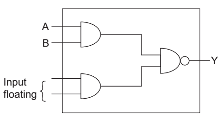
- Figure shows the internal schematic of TTL IC, for the input shown, output Y is—
-
View Hint View Answer Discuss in Forum
When inputs are floating, assume floating input/ inputs should be equal to 1. So, Y = 1. AB = AB
Correct Option: D
When inputs are floating, assume floating input/ inputs should be equal to 1. So, Y = 1. AB = AB

